Intrinsic qualities define the core value or nature of something, reflecting its essential characteristics rather than external attributes. Understanding intrinsic properties can help you make more informed decisions about products, relationships, or personal growth. Discover how intrinsic factors influence various aspects of life by reading the rest of the article.
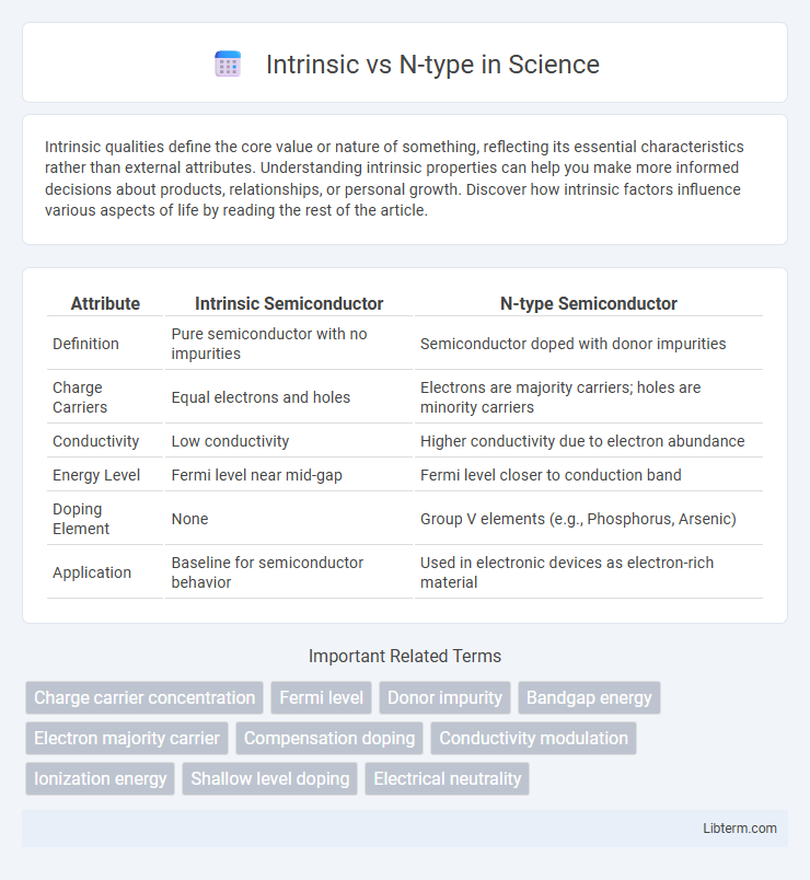
Table of Comparison
| Attribute | Intrinsic Semiconductor | N-type Semiconductor |
|---|---|---|
| Definition | Pure semiconductor with no impurities | Semiconductor doped with donor impurities |
| Charge Carriers | Equal electrons and holes | Electrons are majority carriers; holes are minority carriers |
| Conductivity | Low conductivity | Higher conductivity due to electron abundance |
| Energy Level | Fermi level near mid-gap | Fermi level closer to conduction band |
| Doping Element | None | Group V elements (e.g., Phosphorus, Arsenic) |
| Application | Baseline for semiconductor behavior | Used in electronic devices as electron-rich material |
Introduction to Intrinsic and N-Type Semiconductors
Intrinsic semiconductors are pure materials, such as silicon or germanium, with no significant impurities, exhibiting electrical conductivity primarily due to thermally generated electron-hole pairs. N-type semiconductors result from doping intrinsic semiconductors with pentavalent elements like phosphorus or arsenic, introducing extra electrons that serve as majority charge carriers. This doping process enhances conductivity by increasing free electron concentration, creating distinct electronic properties essential for semiconductor device applications.
Fundamental Differences Between Intrinsic and N-Type
Intrinsic semiconductors consist of pure materials like silicon or germanium without any significant impurities, exhibiting equal concentrations of electrons and holes. N-type semiconductors result from doping intrinsic materials with pentavalent elements such as phosphorus, which introduce excess free electrons as majority carriers. This fundamental difference leads to higher electrical conductivity in N-type semiconductors due to the abundance of electron charge carriers compared to the balanced carrier concentrations in intrinsic materials.
Atomic Structure and Chemical Composition
Intrinsic semiconductors consist of pure silicon or germanium atoms arranged in a crystal lattice with each atom sharing four covalent bonds, resulting in a balanced number of electrons and holes. N-type semiconductors are created by doping the intrinsic material with pentavalent elements such as phosphorus or arsenic, introducing extra electrons as majority charge carriers. This chemical composition alters the atomic structure by adding donor atoms that contribute free electrons, enhancing electrical conductivity.
Electrical Conductivity: Intrinsic vs N-Type
Intrinsic semiconductors exhibit relatively low electrical conductivity due to the limited number of charge carriers generated by thermal excitation alone. N-type semiconductors significantly enhance electrical conductivity by introducing donor impurities, which increase the concentration of free electrons as majority carriers. This doping process reduces resistivity and improves charge transport efficiency in electronic devices.
Role of Impurities in Semiconductor Types
Impurities play a crucial role in defining semiconductor types by altering their electrical properties. Intrinsic semiconductors are pure materials like silicon or germanium with no intentional impurities, exhibiting equal numbers of electrons and holes. N-type semiconductors are created by doping the intrinsic material with pentavalent atoms such as phosphorus or arsenic, which introduce extra electrons, enhancing conductivity by increasing negative charge carriers.
Carrier Concentration and Charge Dynamics
Intrinsic semiconductors exhibit balanced electron and hole concentrations determined by the material's band gap and temperature, with carrier generation primarily through thermal excitation. N-type semiconductors possess a higher electron concentration due to donor impurities introducing additional electrons into the conduction band, significantly enhancing electrical conductivity. Charge dynamics in intrinsic materials involve recombination and generation equilibrium, while n-type doping shifts this balance, reducing hole concentration and increasing free electron mobility for improved charge transport efficiency.
Energy Band Diagrams Comparison
Intrinsic semiconductors have a symmetric energy band diagram with a clear bandgap between the valence band, fully occupied by electrons, and the conduction band, which is empty at absolute zero. N-type semiconductors display an energy band diagram where donor atoms introduce discrete energy levels just below the conduction band, facilitating electron excitation into the conduction band at lower energies. This results in increased electron concentration in the conduction band, reducing the bandgap effect on conductivity compared to intrinsic materials.
Applications of Intrinsic and N-Type Semiconductors
Intrinsic semiconductors are primarily utilized in high-purity and sensitive electronic devices such as photodetectors and infrared sensors due to their balanced electron-hole generation. N-type semiconductors, doped with donor impurities like phosphorus, are widely applied in transistors, diodes, and integrated circuits for enhanced electrical conductivity and faster electron flow. The choice between intrinsic and n-type materials depends on the required electrical characteristics and performance of devices in circuits and optoelectronic applications.
Advantages and Limitations of Each Type
Intrinsic semiconductors offer high purity and minimal impurity interference, providing predictable electrical behavior ideal for fundamental research and precise applications; however, their low conductivity at room temperature limits their efficiency in practical devices. N-type semiconductors, doped with elements like phosphorus or arsenic, exhibit increased conductivity due to excess electrons, enhancing device performance in transistors and diodes, but their electrical properties can degrade over time due to impurity scattering and thermal instability. Choosing between intrinsic and N-type depends on the balance between desired electrical performance and stability requirements in semiconductor device design.
Future Trends in Semiconductor Technology
Future trends in semiconductor technology indicate a shift towards optimizing N-type materials due to their superior electron mobility, which enhances device performance and energy efficiency. Research into intrinsic semiconductors focuses on improving purity and defect control to achieve better baseline electrical properties essential for next-generation nanoelectronics. Advances in doping techniques and material engineering are expected to further narrow the performance gap between intrinsic and N-type semiconductors, enabling more scalable and cost-effective manufacturing processes.
Intrinsic Infographic

 libterm.com