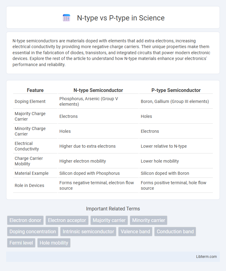
N-type semiconductors are materials doped with elements that add extra electrons, increasing electrical conductivity by providing more negative charge carriers. Their unique properties make them essential in the fabrication of diodes, transistors, and integrated circuits that power modern electronic devices. Explore the rest of the article to understand how N-type materials enhance your electronics' performance and reliability.
Table of Comparison
| Feature | N-type Semiconductor | P-type Semiconductor |
|---|---|---|
| Doping Element | Phosphorus, Arsenic (Group V elements) | Boron, Gallium (Group III elements) |
| Majority Charge Carrier | Electrons | Holes |
| Minority Charge Carrier | Holes | Electrons |
| Electrical Conductivity | Higher due to extra electrons | Lower relative to N-type |
| Charge Carrier Mobility | Higher electron mobility | Lower hole mobility |
| Material Example | Silicon doped with Phosphorus | Silicon doped with Boron |
| Role in Devices | Forms negative terminal, electron flow source | Forms positive terminal, hole flow source |
Introduction to N-type and P-type Semiconductors
N-type semiconductors are created by doping intrinsic semiconductor materials, such as silicon, with pentavalent elements like phosphorus, which introduce extra electrons as charge carriers. P-type semiconductors result from doping with trivalent elements like boron, creating holes that act as positive charge carriers. These fundamental differences in charge carriers define their electrical conductivity and behavior in electronic devices.
Basic Principles of Semiconductor Doping
N-type and P-type semiconductors differ primarily in the type of dopants added to intrinsic silicon to alter its electrical properties. N-type doping introduces pentavalent atoms such as phosphorus, which contribute free electrons as majority carriers, enhancing conductivity. P-type doping involves trivalent atoms like boron, creating "holes" or positive charge carriers that facilitate electrical flow through the semiconductor.
Key Differences Between N-type and P-type Materials
N-type materials contain an excess of electrons as majority charge carriers due to the addition of pentavalent dopants like phosphorus, enhancing electrical conductivity. P-type materials have holes as majority charge carriers, created by doping with trivalent elements such as boron, which accept electrons and create positive charge carriers. The key difference lies in the type of charge carrier and dopant used, influencing the electrical behavior and application in semiconductor devices like diodes and transistors.
Common Dopants for N-type and P-type Semiconductors
Common dopants for N-type semiconductors include phosphorus, arsenic, and antimony, which introduce extra electrons as charge carriers. For P-type semiconductors, boron, gallium, and indium are widely used dopants that create holes by accepting electrons. These dopants significantly alter the electrical conductivity and carrier concentration in silicon-based semiconductor devices.
Electrical Conductivity: N-type vs P-type
N-type semiconductors exhibit higher electrical conductivity due to the abundance of free electrons acting as charge carriers, while P-type semiconductors have holes as the majority carriers, resulting in comparatively lower conductivity. The doping of N-type materials with pentavalent atoms introduces extra electrons, which increases electron mobility, whereas P-type doping with trivalent atoms creates holes that facilitate current flow but generally offer less mobility than electrons. This fundamental difference in charge carrier type directly impacts the performance and efficiency of electronic devices utilizing these semiconductors.
Band Structure Comparison
N-type semiconductors feature donor energy levels close to the conduction band, facilitating electron excitation with minimal energy input and resulting in high electron mobility. P-type semiconductors contain acceptor levels near the valence band, which create holes that act as positive charge carriers with higher effective mass and lower mobility compared to electrons. The band structure difference between N-type and P-type materials directly influences charge carrier concentration and conductivity, critical for optimizing electronic device performance.
Role in PN Junctions and Diodes
N-type semiconductors contain an abundance of electrons acting as majority carriers, which diffuse across the PN junction to recombine with holes from the P-type side. P-type semiconductors have holes as majority carriers that facilitate current flow by accepting electrons at the junction, creating a depletion region crucial for diode operation. The interaction between N-type and P-type materials forms the rectifying behavior of diodes, enabling controlled current conduction and blocking in reverse bias conditions.
Applications in Modern Electronics
N-type semiconductors, enriched with electrons as majority carriers, are essential in creating high-speed transistors and diodes used in digital circuits and power electronics. P-type semiconductors, characterized by holes as majority carriers, play a crucial role in forming p-n junctions, which are fundamental components in solar cells, LEDs, and bipolar junction transistors (BJTs). The combination of N-type and P-type materials enables the design of integrated circuits, enabling efficient switching, amplification, and energy conversion in modern electronic devices.
Advantages and Limitations of Each Type
N-type semiconductors offer high electron mobility, resulting in faster electrical conductivity and lower resistivity, making them ideal for high-speed electronic devices. However, their performance can be limited by electron recombination rates and potential instability under certain environmental conditions. P-type semiconductors provide better hole mobility and are often more stable in oxidizing environments, but they exhibit slower charge carrier movement and higher resistivity compared to N-type materials.
Future Trends in Semiconductor Technology
Future trends in semiconductor technology emphasize advancements in N-type and P-type materials to enhance device performance and energy efficiency. Innovations in doping techniques and the development of novel compound semiconductors like gallium nitride (GaN) and silicon carbide (SiC) focus on optimizing electron mobility in N-type and hole mobility in P-type regions. Research on complementary metal-oxide-semiconductor (CMOS) scaling relies heavily on balancing N-type and P-type transistor enhancements to sustain Moore's Law and enable next-generation integrated circuits.
N-type Infographic

 libterm.com