Lattice mismatch occurs when two materials with different lattice constants are joined, leading to strain and dislocations at the interface. This phenomenon significantly impacts the performance of semiconductor devices and the quality of thin films in nanotechnology applications. Discover how understanding lattice mismatch can improve Your material design and device fabrication by reading the full article.
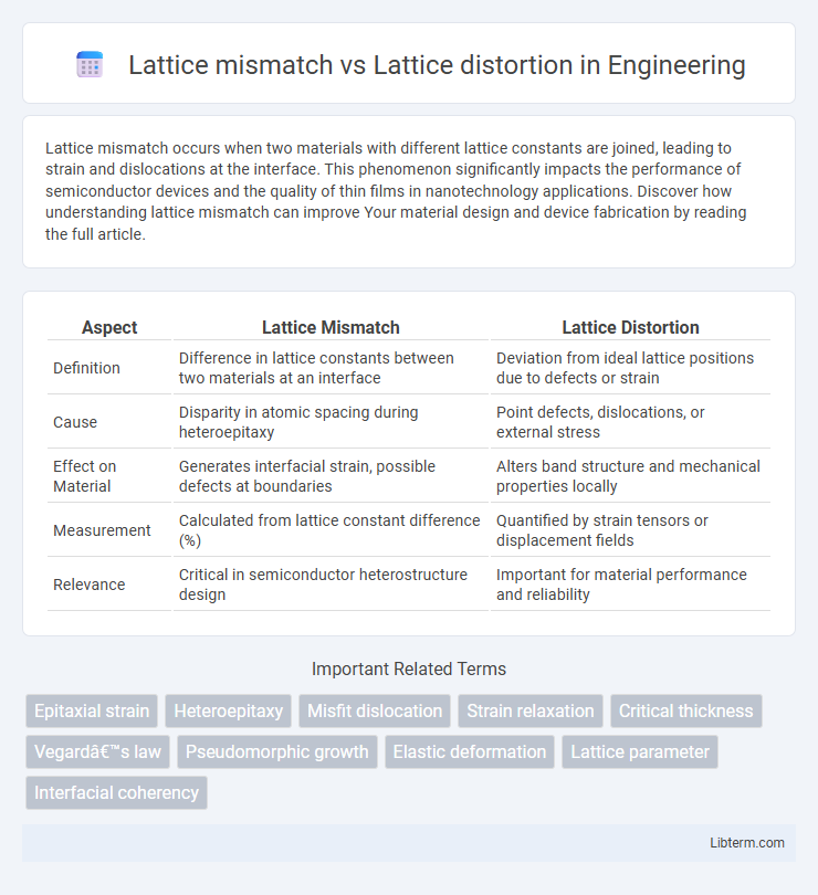
Table of Comparison
| Aspect | Lattice Mismatch | Lattice Distortion |
|---|---|---|
| Definition | Difference in lattice constants between two materials at an interface | Deviation from ideal lattice positions due to defects or strain |
| Cause | Disparity in atomic spacing during heteroepitaxy | Point defects, dislocations, or external stress |
| Effect on Material | Generates interfacial strain, possible defects at boundaries | Alters band structure and mechanical properties locally |
| Measurement | Calculated from lattice constant difference (%) | Quantified by strain tensors or displacement fields |
| Relevance | Critical in semiconductor heterostructure design | Important for material performance and reliability |
Introduction to Lattice Mismatch and Lattice Distortion
Lattice mismatch occurs when two crystalline materials with different lattice constants are joined, causing strain at the interface due to the discrepancy in atomic spacing. Lattice distortion refers to deviations from the ideal crystal lattice structure, resulting from defects, strain, or external influences that alter atomic positions. Understanding lattice mismatch is crucial for controlling strain-induced lattice distortion, which significantly impacts the electronic and mechanical properties of materials.
Definitions: Lattice Mismatch vs. Lattice Distortion
Lattice mismatch refers to the difference in lattice constants or atomic spacing between two materials when they are joined, often occurring at heterojunction interfaces in semiconductor devices. Lattice distortion involves the alteration or deformation of the original lattice structure due to external stresses or incorporation of dopants, resulting in strain and defects within the crystal. Understanding the distinction between lattice mismatch, which is an interfacial property, and lattice distortion, a localized structural change, is critical for optimizing material performance in epitaxial growth and device fabrication.
Causes of Lattice Mismatch
Lattice mismatch occurs when two crystalline materials with different lattice constants are joined, leading to strain due to the difference in atomic spacing. Causes of lattice mismatch include differences in chemical composition, temperature variations during growth, and defects at the interface, which prevent perfect lattice alignment. Lattice distortion results from the relaxation of this strain, causing changes in bond angles and lengths within the crystal structure.
Origins of Lattice Distortion
Lattice distortion originates from defects, impurities, and external stresses causing deviations in the ideal crystalline arrangement, distinct from lattice mismatch which refers to the difference in lattice constants between two materials. Point defects, dislocations, and substitutional atoms introduce strain fields that alter interatomic distances, leading to local lattice distortions. These distortions influence mechanical, electronic, and optical properties by modifying the crystal symmetry and bond angles within the host lattice.
Measurement Techniques for Lattice Mismatch
Lattice mismatch quantifies the difference in lattice parameters between two crystalline materials, often measured through high-resolution X-ray diffraction (HRXRD) by analyzing peak shifts and strain profiles. Lattice distortion refers to local deviations in atomic positions caused by defects or strain and is typically assessed using transmission electron microscopy (TEM) for atomic-scale imaging. Advanced techniques such as reciprocal space mapping (RSM) complement HRXRD by providing detailed strain distribution, offering precise measurement of lattice mismatch in heteroepitaxial layers.
Methods for Analyzing Lattice Distortion
Lattice mismatch refers to the difference in lattice parameters between two adjoining crystalline materials, often causing strain at the interface. Methods for analyzing lattice distortion include high-resolution X-ray diffraction (HRXRD) to quantify strain and dislocation density, transmission electron microscopy (TEM) for direct imaging of defects and lattice distortions, and Raman spectroscopy to detect shifts in vibrational modes indicative of strain. These techniques provide detailed insights into the extent and nature of lattice distortions resulting from mismatch in heteroepitaxial layers.
Effects of Lattice Mismatch on Material Properties
Lattice mismatch occurs when two materials with different lattice constants are joined, leading to strain and defects at the interface that significantly influence electronic, optical, and mechanical properties. This mismatch induces lattice distortion, which can alter carrier mobility, increase dislocation density, and modify band structure, affecting the performance of semiconductor devices and heterostructures. Managing lattice mismatch is critical for optimizing material quality and enhancing device efficiency in applications such as epitaxial growth and thin-film technology.
Impact of Lattice Distortion on Crystal Structure
Lattice distortion significantly alters the crystal structure by introducing strain and defects that disrupt the ideal periodic arrangement of atoms. This distortion affects material properties such as electronic band structure, mechanical strength, and thermal conductivity by creating localized variations in atomic spacing. Unlike lattice mismatch, which refers to the difference in lattice parameters between two materials, lattice distortion specifically pertains to the internal deviations within the crystal lattice caused by external stresses or impurities.
Applications Influenced by Lattice Mismatch and Distortion
Lattice mismatch occurs when two materials with different lattice constants form an interface, causing strain that can alter electronic and optical properties essential for semiconductor devices and heterostructures. Lattice distortion refers to local deviations in the crystal lattice, impacting material strength, defect generation, and carrier mobility, which are critical in catalyst design and flexible electronics. Applications such as quantum wells, superlattices, and solar cells rely heavily on controlled lattice mismatch and distortion to optimize performance and durability.
Comparative Analysis: Lattice Mismatch vs. Lattice Distortion
Lattice mismatch refers to the difference in lattice parameters between two adjoining crystalline materials, often quantified as a percentage, which primarily affects the formation of interfaces and heterostructures. Lattice distortion, on the other hand, involves the strain or modification within the lattice caused by defects, impurities, or external stresses, affecting the atomic arrangement locally or uniformly. Comparative analysis reveals that lattice mismatch predominantly influences interface quality and epitaxial growth, while lattice distortion governs material properties such as electronic band structure and mechanical strength within the crystal.
Lattice mismatch Infographic