Hold time refers to the duration a caller must wait on the line before reaching a customer service representative or completing an automated process. Minimizing hold time improves customer satisfaction and enhances overall service efficiency. Discover how effective hold time management can transform Your customer experience in the rest of this article.
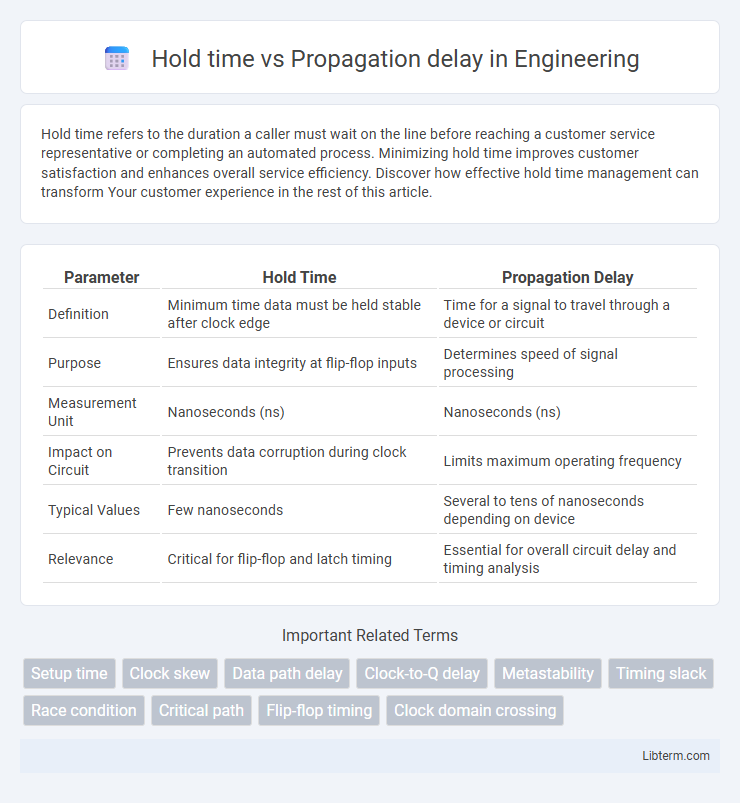
Table of Comparison
| Parameter | Hold Time | Propagation Delay |
|---|---|---|
| Definition | Minimum time data must be held stable after clock edge | Time for a signal to travel through a device or circuit |
| Purpose | Ensures data integrity at flip-flop inputs | Determines speed of signal processing |
| Measurement Unit | Nanoseconds (ns) | Nanoseconds (ns) |
| Impact on Circuit | Prevents data corruption during clock transition | Limits maximum operating frequency |
| Typical Values | Few nanoseconds | Several to tens of nanoseconds depending on device |
| Relevance | Critical for flip-flop and latch timing | Essential for overall circuit delay and timing analysis |
Introduction to Hold Time and Propagation Delay
Hold time is the minimum period after a clock edge during which data must remain stable to ensure correct latch or flip-flop operation, preventing data corruption. Propagation delay refers to the time it takes for a signal to travel through a digital circuit component, from input to output, affecting overall system timing and synchronization. Understanding the relationship between hold time and propagation delay is critical for designing reliable synchronous digital systems and avoiding timing violations.
Defining Hold Time in Digital Circuits
Hold time in digital circuits is the minimum duration a data input must remain stable after the clock edge to ensure proper data capture by a flip-flop or latch. It prevents data corruption by ensuring the sequential element captures the correct input state before it changes. Propagation delay, by contrast, refers to the time taken for a signal to travel through a circuit element, influencing timing constraints but distinct from hold time requirements.
Understanding Propagation Delay
Propagation delay refers to the time it takes for a signal to travel from the input of a digital circuit to its output, affecting the overall speed and timing accuracy of the system. This delay is influenced by physical factors such as the length and material of the interconnecting wires, transistor switching speeds, and the capacitance of the circuit elements. Understanding propagation delay is essential for designing reliable synchronous circuits where timing margins must accommodate this delay to prevent setup and hold time violations.
Key Differences Between Hold Time and Propagation Delay
Hold time is the minimum period after the clock edge during which the data input must remain stable to ensure correct latching, while propagation delay is the time taken for a signal to travel from the input to the output of a digital circuit. Hold time is critical for maintaining data integrity within flip-flops and latches, whereas propagation delay impacts the overall speed and timing of signal transmission in combinational logic. The key difference lies in hold time being a stability requirement post-clock edge, whereas propagation delay measures signal travel time through circuit elements.
Importance of Hold Time in Timing Analysis
Hold time is the minimum duration after a clock edge during which the data input must remain stable to ensure correct latch or flip-flop operation, preventing data corruption in synchronous circuits. Propagation delay represents the time taken for a signal to travel through a circuit element, influencing the overall timing budget but not the immediate data stability. Emphasizing hold time in timing analysis is crucial for avoiding timing violations that can cause metastability, ensuring reliable data capture and system stability in high-speed digital designs.
Role of Propagation Delay in Signal Integrity
Propagation delay determines the time it takes for a signal to travel through a circuit, directly impacting signal integrity by influencing the timing margin available for reliable data capture. Insufficient propagation delay can cause signals to arrive before the clock edge, violating hold time requirements and leading to data corruption or metastability in synchronous systems. Designing circuits with appropriate propagation delays ensures signals are stable and valid at flip-flop inputs, maintaining robust timing and minimizing errors in high-speed digital systems.
Common Causes of Hold Time Violations
Hold time violations often stem from variations in clock skew, data path delays, and load capacitance, which disrupt the timing relationship between clock and data signals. Insufficient delay elements or overly fast data transitions can cause data to change before the latch or flip-flop reliably captures it, leading to hold time failures. Common design issues include inadequate buffering, improper clock distribution, and process variations affecting transistor speed, all contributing to propagation delays that interfere with hold time requirements.
Effects of Propagation Delay on Circuit Performance
Propagation delay significantly impacts circuit performance by causing timing mismatches between signals, which can lead to data corruption or setup and hold time violations. Longer propagation delays reduce the maximum operating frequency of digital circuits, limiting overall system speed and efficiency. In synchronous systems, improper handling of propagation delay results in metastability and unreliable data transfer between sequential logic elements.
Techniques to Mitigate Hold Time and Propagation Delay Issues
Hold time violations and propagation delay challenges in digital circuits can be mitigated using techniques such as clock skew adjustment, where intentional delay is introduced to synchronize signal arrival times. Implementing delay buffers or re-timing registers helps to balance data path delays and ensure stable data sampling. Employing advanced clock distribution methods and optimizing logic paths further reduces the risks of timing violations, enhancing overall circuit reliability.
Conclusion: Balancing Hold Time and Propagation Delay for Reliable Designs
Balancing hold time and propagation delay is crucial for reliable digital circuit designs, as insufficient hold time can cause data corruption while excessive propagation delay may reduce system performance. Designers must carefully optimize clock timing and data path latencies to ensure setup and hold constraints are met simultaneously. Achieving this balance enhances signal integrity, prevents metastability, and ensures consistent operation across different process variations and environmental conditions.
Hold time Infographic